- 您现在的位置:买卖IC网 > Sheet目录1992 > DAC8413EP (Analog Devices Inc)IC DAC 12BIT QUAD V-OUT 28-DIP
Data Sheet
DAC8412/DAC8413
Rev. G | Page 5 of 20
Parameter
Symbol
Conditions
Min
Typ
Max
Units
Write Data Setup
tWDS
tWCS = 150 ns
20
ns
Write Data Hold
tWDH
tWCS = 150 ns
0
ns
Load Data Pulse Width
tLDW
180
ns
Reset Pulse Width
tRESET
150
ns
Chip Select Read Pulse Width
tRCS
170
ns
Read Data Hold
tRDH
tRCS = 170 ns
20
ns
Read Data Setup
tRDS
tRCS = 170 ns
0
ns
Data to High-Z
tDZ
CL = 10 pF
200
ns
Chip Select to Data
tCSD
CL = 100 pF
320
ns
SUPPLY CHARACTERISTICS
Power Supply Sensitivity
PSS
100
ppm/V
Positive Supply Current
IDD
7
12
mA
Negative Supply Current
ISS
VSS = 5.0 V
10
mA
Power Dissipation
PDISS
VSS = 0 V
60
mW
VSS = 5.0 V
110
mW
1 All supplies can be varied ±5%, and operation is guaranteed. Device is tested with VDD = 4.75 V.
2 For single-supply operation only (VREFL = 0.0 V, VSS = 0.0 V). Due to internal offset errors, INL and DNL are measured beginning at 0x005.
3 Operation is guaranteed over this reference range, but linearity is neither tested nor guaranteed.
4 All parameters are guaranteed by design.
5 All input control signals are specified with tr = tf = 5 ns (10% to 90% of 5 V) and timed from a voltage level of 1.6 V.
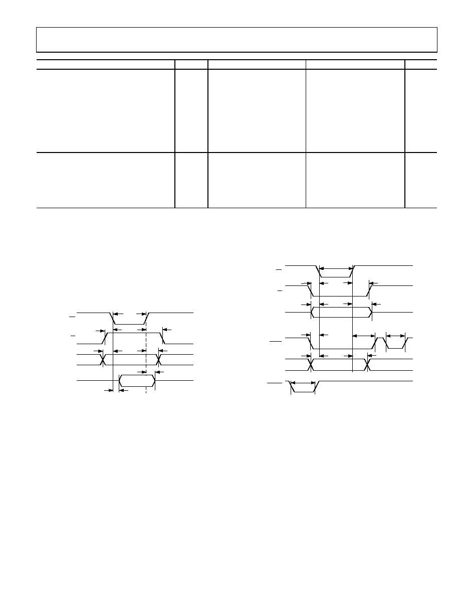
CS
A0/A1
tRDS
tRCS
tRDH
tAS
tAH
tDZ
tCSD
R/W
DATA
OUT
DATA VALID
HIGH-Z
00
27
4-
00
3
Figure 3. Data Output (Read Timing)
A0/A1
RESET
LDAC
tWCS
R/W
CS
DATA IN
tWS
tWH
tAS
tAH
tLS
tLH
tWDH
tWDS
tLDW
tRESET
00
27
4-
0
04
Figure 4. Data Write (Input and Output Registers) Timing
发布紧急采购,3分钟左右您将得到回复。
相关PDF资料
DAC8420FQ
IC DAC 12BIT QUAD SRL LP 16-CDIP
DAC8426EPZ
IC DAC 8BIT QUAD 10VREF 20PDIP
DAC8531IDRBTG4
IC D/A CONV LP 16-BIT 8-SON
DAC8562FP
IC DAC 12BIT PARALLEL 5V 20-DIP
DS1004Z-5+T
IC DELAY LINE 5TAP 25NS 8-SOIC
DS1005-125+
IC DELAY LINE 5TAP 125NS 14-DIP
DS1007S-2+T&R
IC DELAY LINE 4NS 16-SOIC
DS1010S-50+T&R
IC DELAY LINE 10TAP 16-SOIC
相关代理商/技术参数
DAC8413EPZ
功能描述:IC DAC 12BIT QUAD V-OUT 28DIP RoHS:是 类别:集成电路 (IC) >> 数据采集 - 数模转换器 系列:- 产品培训模块:Lead (SnPb) Finish for COTS
Obsolescence Mitigation Program 标准包装:1,000 系列:- 设置时间:1µs 位数:8 数据接口:串行 转换器数目:8 电压电源:双 ± 功率耗散(最大):941mW 工作温度:0°C ~ 70°C 安装类型:表面贴装 封装/外壳:24-SOIC(0.295",7.50mm 宽) 供应商设备封装:24-SOIC W 包装:带卷 (TR) 输出数目和类型:8 电压,单极 采样率(每秒):*
DAC8413FP
功能描述:IC DAC 12BIT QUAD V-OUT 28-DIP RoHS:否 类别:集成电路 (IC) >> 数据采集 - 数模转换器 系列:- 产品培训模块:Lead (SnPb) Finish for COTS
Obsolescence Mitigation Program 标准包装:1,000 系列:- 设置时间:1µs 位数:8 数据接口:串行 转换器数目:8 电压电源:双 ± 功率耗散(最大):941mW 工作温度:0°C ~ 70°C 安装类型:表面贴装 封装/外壳:24-SOIC(0.295",7.50mm 宽) 供应商设备封装:24-SOIC W 包装:带卷 (TR) 输出数目和类型:8 电压,单极 采样率(每秒):*
DAC8413FPC
功能描述:IC DAC 12BIT QUAD READBK 28-PLCC RoHS:否 类别:集成电路 (IC) >> 数据采集 - 数模转换器 系列:- 产品培训模块:Lead (SnPb) Finish for COTS
Obsolescence Mitigation Program 标准包装:1,000 系列:- 设置时间:1µs 位数:8 数据接口:串行 转换器数目:8 电压电源:双 ± 功率耗散(最大):941mW 工作温度:0°C ~ 70°C 安装类型:表面贴装 封装/外壳:24-SOIC(0.295",7.50mm 宽) 供应商设备封装:24-SOIC W 包装:带卷 (TR) 输出数目和类型:8 电压,单极 采样率(每秒):*
DAC8413FPC-REEL
功能描述:IC DAC 12BIT QUAD V-OUT 28-PLCC RoHS:否 类别:集成电路 (IC) >> 数据采集 - 数模转换器 系列:- 产品培训模块:Data Converter Fundamentals
DAC Architectures 标准包装:750 系列:- 设置时间:7µs 位数:16 数据接口:并联 转换器数目:1 电压电源:双 ± 功率耗散(最大):100mW 工作温度:0°C ~ 70°C 安装类型:表面贴装 封装/外壳:28-LCC(J 形引线) 供应商设备封装:28-PLCC(11.51x11.51) 包装:带卷 (TR) 输出数目和类型:1 电压,单极;1 电压,双极 采样率(每秒):143k
DAC8413FPCZ
功能描述:IC DAC 12BIT QUAD READBK 28-PLCC RoHS:是 类别:集成电路 (IC) >> 数据采集 - 数模转换器 系列:- 产品培训模块:Lead (SnPb) Finish for COTS
Obsolescence Mitigation Program 标准包装:1,000 系列:- 设置时间:1µs 位数:8 数据接口:串行 转换器数目:8 电压电源:双 ± 功率耗散(最大):941mW 工作温度:0°C ~ 70°C 安装类型:表面贴装 封装/外壳:24-SOIC(0.295",7.50mm 宽) 供应商设备封装:24-SOIC W 包装:带卷 (TR) 输出数目和类型:8 电压,单极 采样率(每秒):*
DAC8413FPCZ-REEL
功能描述:IC DAC 12BIT QUAD V-OUT 28PLCC RoHS:是 类别:集成电路 (IC) >> 数据采集 - 数模转换器 系列:- 产品培训模块:Data Converter Fundamentals
DAC Architectures 标准包装:750 系列:- 设置时间:7µs 位数:16 数据接口:并联 转换器数目:1 电压电源:双 ± 功率耗散(最大):100mW 工作温度:0°C ~ 70°C 安装类型:表面贴装 封装/外壳:28-LCC(J 形引线) 供应商设备封装:28-PLCC(11.51x11.51) 包装:带卷 (TR) 输出数目和类型:1 电压,单极;1 电压,双极 采样率(每秒):143k
DAC8413FPZ
功能描述:IC DAC 12BIT QUAD V-OUT 28DIP RoHS:是 类别:集成电路 (IC) >> 数据采集 - 数模转换器 系列:- 标准包装:1 系列:- 设置时间:4.5µs 位数:12 数据接口:串行,SPI? 转换器数目:1 电压电源:单电源 功率耗散(最大):- 工作温度:-40°C ~ 125°C 安装类型:表面贴装 封装/外壳:8-SOIC(0.154",3.90mm 宽) 供应商设备封装:8-SOICN 包装:剪切带 (CT) 输出数目和类型:1 电压,单极;1 电压,双极 采样率(每秒):* 其它名称:MCP4921T-E/SNCTMCP4921T-E/SNRCTMCP4921T-E/SNRCT-ND
dac8413ft
制造商:Rochester Electronics LLC 功能描述:- Bulk 制造商:Analog Devices 功能描述: